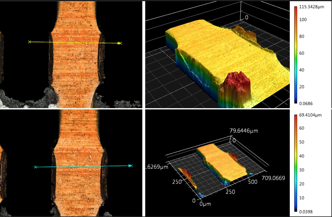
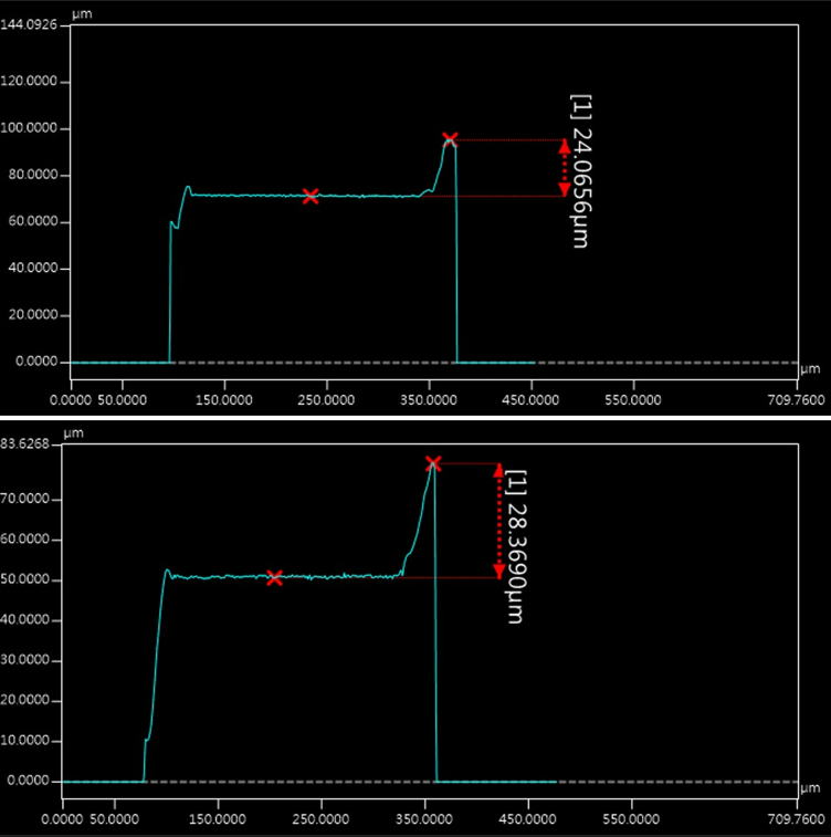
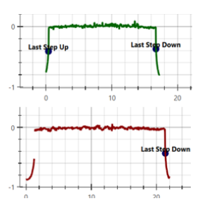
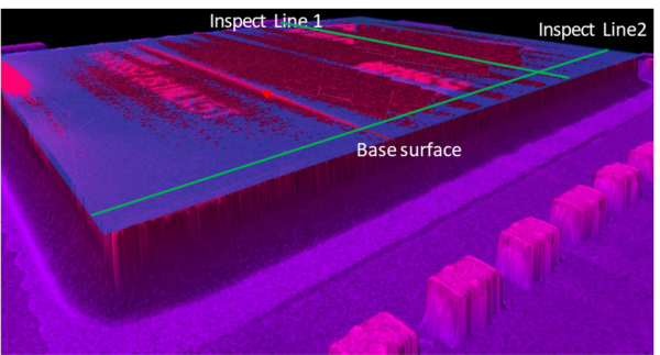
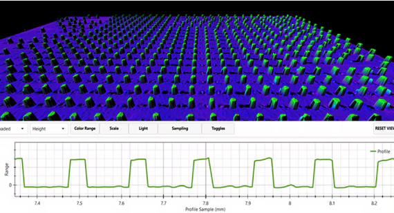
半導體 3D檢量測系統 3D檢量測系統興城提供不同精度的3D檢量測方案,提供半導體與封裝製程中,任何需要進行3D檢測的缺陷。系統特性超高解析度與高產能檢測 ( 可依客戶規格要求客製 )3 μm 級 Z 軸解析,符合高標準製程即時檢測,防止良率損失數據精準量化,降低誤判檢測表面缺陷 3D 輪廓,搭配 Profile 曲線呈現AI 智能判別選配,強化自動化檢測客製化設備結構配置規劃適用場域測量 Underfill 點膠寬度、高度與流動性,支援周邊與被動元件同步檢查翹曲檢查Wire Bond 線寬、弧高Bump 高度、尺寸、平整度SMT 立碑、Shift、缺件異常Socket 異常、錫附著、磨耗偵測任何立體物件之檢量測 High Accuracy 3D Underfill Measurement 3D Inspection SystemWe offer a range of high-precision 3D inspection solutions for semiconductorsand OSATs to meet any 3D inspection need in production.System Features:Ultra-high resolution and high throughput detection (customizable to meet customer standards)3μm Z-axis resolution can meet advanced process requirementsReal-time detection to prevent defects in the processQuantitative data analysis to reduce false positives3D surface defect detection provides contour dataUse AI to assist defect classification to enhance auto-InspectionCustomizable device configurations and layoutsapplication:Underfill width, height and fluidity of the bottom fill dispensing, and Inspection of surrounding componentswarpage detectionWire bond height and radian inspectionBump height, size and coplanaritySMT passive component tombstones / billboards and shift inspectionSocket pin abnormality, tin loss, and wear detectionMeasurement of any 3D object========================